40 consider the circuit diagram in the figure
Consider the circuit diagram depicted in the figure. a. What equation do you get when you apply the loop rule to the abcdefgha, in terms of the variables in the figure? Consider the timing diagram in Figure P7.1. Assuming that the D and Clock inputs shown are applied to the circuit in Figure 7.12, draw waveforms for the Qa, Qb, and Qc signals. P2. (10 points) 7.4 . Show a circuit that implements the gated SR latch using NAND gates only. P3. (15 points) 7.9 . Consider the circuit in Figure P7.2.
(b) The circuit diagram shows the shows battery as an emf source and an internal resistor. The two emf sources have identical emfs (each labeled by ) connected in parallel that produce the same emf. Consider the Kirchhoff analysis of the circuit in (Figure) (b).
Consider the circuit diagram in the figure
Example IV-1. Consider the circuit shown below, where R1 = 3.00 Ω, R2 = 10.0 Ω, R3 = 5.00 Ω, R4 = 4.00 Ω, and R5 = 3.00 Ω. (a) Find the equivalent resistance of this circuit. (b) If the total power supplied to the circuit is 4.00 W, find the emf of the battery. + − E R1 R2 R3 R4 R5 Solution (a): We have to reduce this circuit in steps ... Consider the circuit shown in Figure P5.12. Find the phasors I, IR, and Ic. Construct the phasor diagram. 10 mH 100 cos (10ʻr) 100 2 1 µF iR. check_circle. Consider the electrical circuit shown in Figure 3-85, Obtain the transfer function Es)/E(s) by use of the block diagram approach. ww Figure 3-85 Electrical circuit.
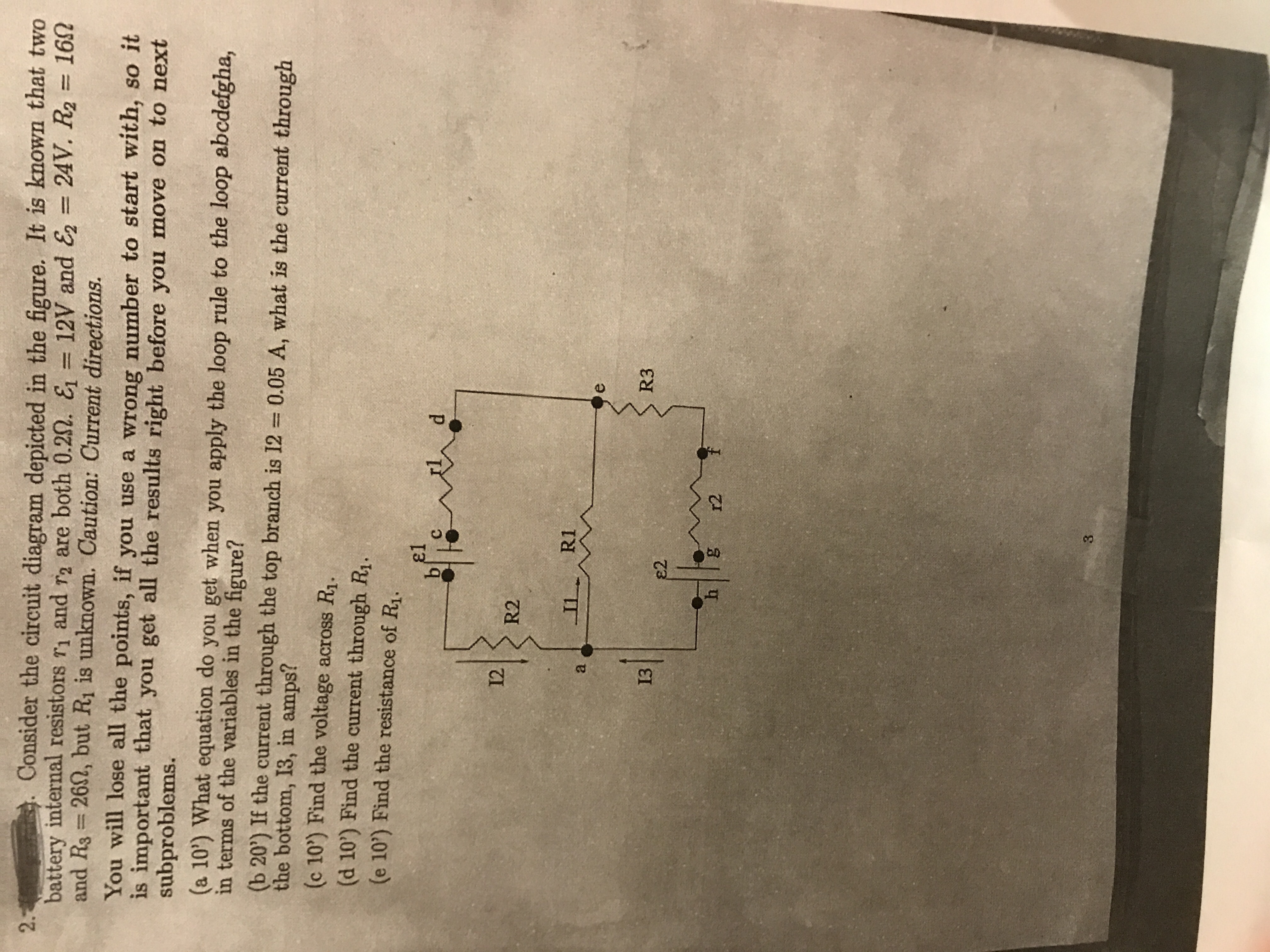
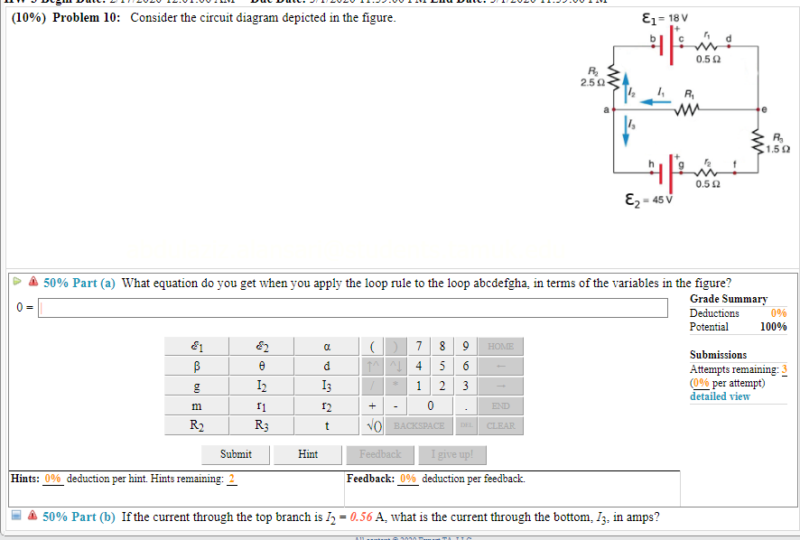
Consider the circuit diagram in the figure. Figure 6.13. State-assigned table for the sequential circuit in Figure 6.12. Present Next state state Outputs A 00 00 0 1 0 0 0 0 0 0 0 B 01 10 1 0 0 0 1 0 0 1 0 C 10 11 1 1 1 0 0 1 0 0 0 D 11 00 0 0 0 1 0 0 1 0 1 7.1 Consider the timing diagram in Figure P7.1. Assuming that the D and Clock inputs shown are applied to the circuit in Figure 7.12, draw the waveforms for the Qa, Qb, Qc signals. 7.5 Given a 100-MHz clock signal, derive a circuit using D FF to generate 50-MHz and 25-MHz clock signals. Draw a timing diagram for all three clock signals, assuming Consider the circuit diagram depicted in the fgure. Consider the circuit diagram depicted in the figure. It is known that two battery internal resistors r1and r2 are both 02ω 12v and 24v. Figure 3 the circuit considered in example 2. And rs 262 but ri is unknown. This time the voltage across each of these elements of the circuit is the same. We will use the circuit of Figure 1 for a step by step demonstration of the node method. Figure 2 shows the implementation of steps 1 and 2. We have labeled all elements and identified all relevant nodes in the circuit. R1 R2 R3 R4 Vs + _ n1 n2 n3 n4 Figure 2. Circuit with labeled nodes. The third step is to select one of the identified nodes ...
Such a circuit is called a multiple-input AND-gate and is represented by the diagram shown in Figure 2.4.6. Multiple-input OR-gates are constructed similarly. The Circuit Corresponding to a Boolean Expression Figure 2.4.6 a Given Input/Output Table ==> Circuit Design a circuit for the following input/output table: Consider the circuit shown in the figure below. Find (a) the potential difference between points a and b and (b) the current in the 20.0-V resistor. Consider the circuit shown in the figure below where c1 400 µf c2 700 µf and δv 180 v. 180 v v r 4 400 r 1 200 r 2 300 3 100 label the voltage v 180 v and the resistors. Calculate the power delivered to each resistor in the circuit shown in figure p2131. Consider the following circuit diagram. book Solutions ANSWER Step 0 Refer to figure 9.60 for the circuit diagram in the textbook. Let consider rotor equivalent induced emf as a reference phasor. Write the value of impedance per phase of the inner cage of a double cage induction motor.
Consider the phasor diagram shown in Figure 34.11. The phasor labeled I indicates the current in the circuit. The voltages across the inductor and the capacitor are 90 degrees out of phase with the current and are indicated in Figure 34.11 by the phasors labeled V L and V C . The figure shows a circuit that illustrates the concept of loops, ... Consider the network of four resistors shown in the diagram, where = 2.00 , = 5.00 , = 1.00 , and = 7.00 . The resistors are connected to a constant voltage of magnitude . View solution. >. In Figure a, resistor 3 is a variable resistor and the ideal battery has emf E = 1 2. 0 V. Figure b gives the current i through the battery as a function of R 3 . The horizontal scale is set by R 3 s = 2 0 Ω .The curve has an asymptote of 2.0 mA as R 3 → ∞ ,.What are (a) resistance R 1 and (b) resistance R 2 ? Consider the circuit diagram depicted in the figure. Now apply the loop rule to loop 1 the larger loop spanning the entire circuit. Assume that v 128 v r1 r2 r3 r4 r5 200 ω. B if the current through the top branch is i 2 0605 a. Consider a series rc circuit as in the figure below for which r 100 mω c 500 µf and ε 300 v.
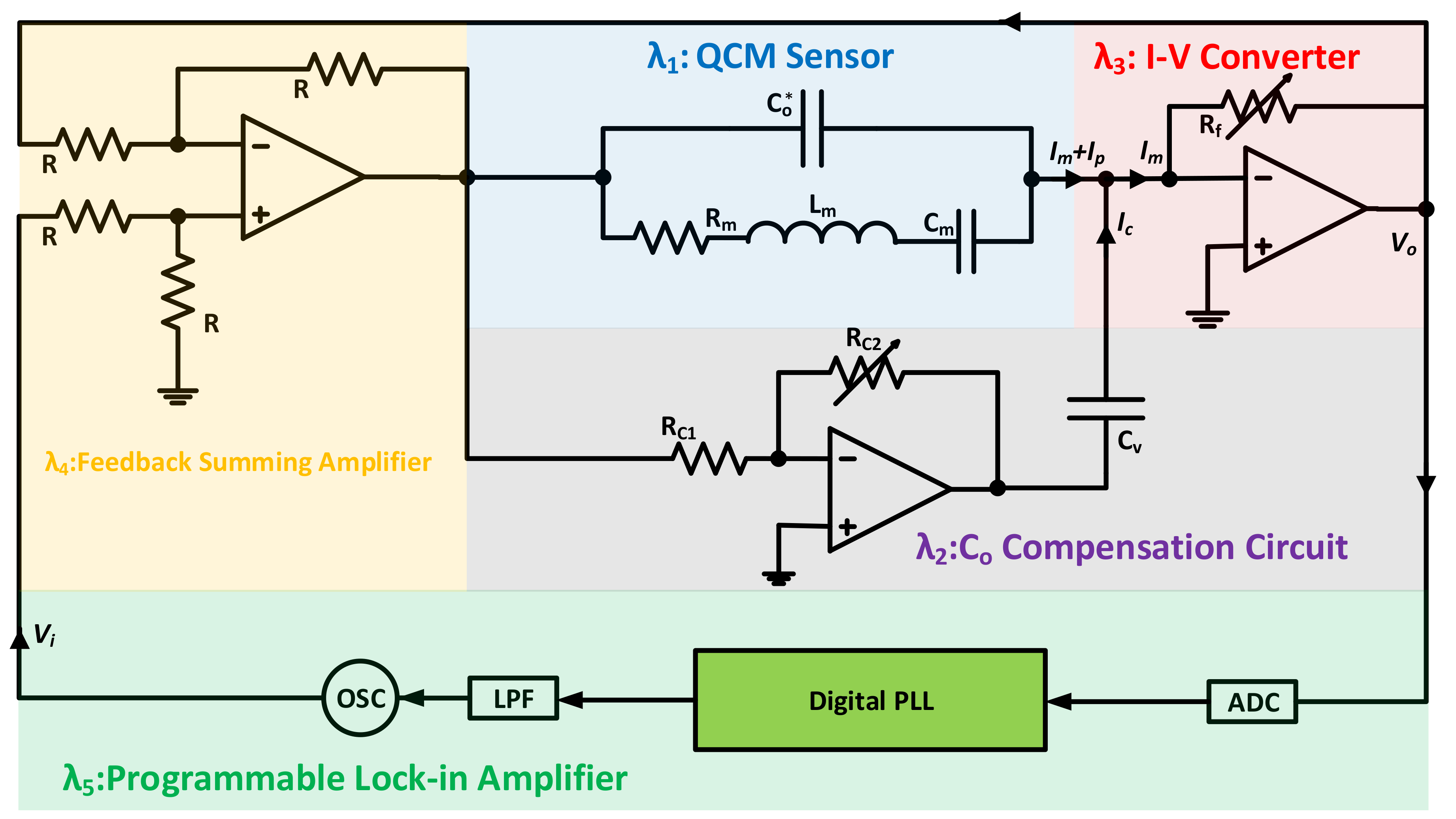
Sensors Free Full Text Quartz Crystal Microbalance Electronic Interfacing Systems A Review Html
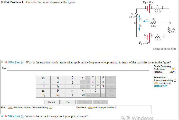
Transcribed image text: (25%) Problem 2: Consider the circuit diagram in the figure 0.5 2 2.512 2 R 6.0 ? 1.5? 0.5 ? Otheexpertta.com × 50% Part (a) what is the equation which results when applying the loop rule to loop aedcba, in terms of the variables given in the figure?

Instrumentation Control Tehnician Axial Vibration
Consider the circuit diagram depicted in the figure. Consider the circuit diagram depicted in the figure. It is known that two 25ω 24v and ε2 36v. What equation do you get when you apply the loop rule to the loop abcdefgha in terms of the variables in the figure. Find the values of the voltage vc and the current ib.

Consider The Four Circuits Shown In The Figure Below In Which Circuit Power Dissipated Maximum Neglect Brainly In
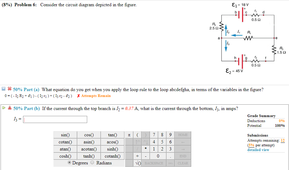
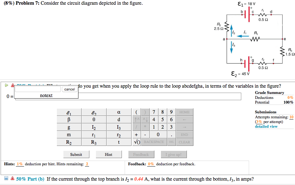
Answer to Solved (6%) Problem 17: Consider the circuit diagram. Transcribed image text: (6%) Problem 17: Consider the circuit diagram depicted in the figure. E1-18V 10.50 359 1050 Ez - 45 A 50% Part (a) What equation do you get when you apply the loop rule to the loop abcdefgha, in terms of the variables in the figure?

Consider The Circuit Shown In The Figure
FREE Expert Solution. 95% (219 ratings) View Complete Written Solution. Problem Details. Consider the circuit shown in the figure below. (Let R = 36.0 Ω.) (a) Find the current in the 36.0-Ω resistor. A. (b) Find the potential difference between points a and b.
Glance Into Solid State Transformer Technology A Mirror For Possible Research Areas Journal Of Applied Materials And Technology
Question: (10%) Problem 5: Consider the circuit diagram depicted in the figure 0.5 Ω R2 2.5 Ω /2 R 1.5Ω 0.5 Ω 50% Part (a) what equation do you get when you apply the loop rule to the loop abcdergha, in terms of the variables in the figure? Grade= 100% Correct Answer Student Final Submission Feedback Correct! 012 R2+ 112 T3 R3 +32-62 0- 1 ...

Draw A Circuit Diagram For The Circuit Of Figure 1 Figure 1 Of 1a Circuit Is Shown In The Figure A 9 Volt Batter Homeworklib
Find step-by-step Physics solutions and your answer to the following textbook question: Consider the portion of a circuit in Figure 17.73. The wire rests on top of the two compasses. When no current is running, both compasses point north (direction shown by the gray arrows). When current runs in the circuit, the needle of compass 1 deflects as shown.
Applied Sciences Free Full Text An Active Clamp Forward Inverter Featuring Soft Switching And Electrical Isolation Html
Figure 3. The loop rule. An example of Kirchhoff's second rule where the sum of the changes in potential around a closed loop must be zero. (a) In this standard schematic of a simple series circuit, the emf supplies 18 V, which is reduced to zero by the resistances, with 1 V across the internal resistance, and 12 V and 5 V across the two load resistances, for a total of 18 V. (b) This ...
Solved 8 Problem 6 Consider The Circuit Diagram Depicted Chegg Com
Consider the circuit diagram depicted in the figure. 0 ω r 3 16. For the action depicted in the figure figure 2 indicate the direction of the induced current in the loop clockwise counterclockwise or zero when seen from the right of the loop. Now consider a diagram describing a parallel ac circuit containing a resistor a capacitor and an inductor.
Consider The Circuit Shown In The Figure The Current I 3 I
The diagram shows a network of four 2 Ω resistors. The effective resistance, in Ω, between X and Y is A 0.5 B 1.2 C 1.7 D 2.0 (Total 1 mark) 1 The circuit shown in ...

An 105 Current Sense Circuit Collection Making Sense Of Current Analog Devices
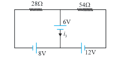
Draw a circuit diagram. R 3 100 v 250 v. Consider the circuit shown in the figure below where c1 400 µf c2 700 µf and δv 180 v. Tactics box 231 using kirchhoffs loop law 1. A find the current flowing through the 5 ω resistor. While kirchhoffs junction law is needed only when there are one or more junctions in a circuit kirchhoffs loop law ...

Best Answer Consider The Following Circuit Diagram If R1 R2 R3 R4 R5 3 Ohm Find Equivalent Brainly In
Consider the circuit diagram depicted in the fgure. It is known that two battery internal resistors r1and r2 are both 0.2Ω· = 12V and & = 24V. R2 16Ω 2. and Rs 262, but Ri is unknown. Caution: Current directions.
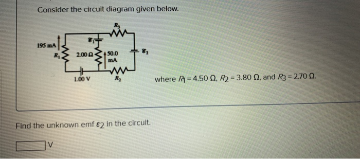
Solved Consider The Circuit Diagram Given Below 195 Ma 2 00 Chegg Com
Consider the electrical circuit shown in Figure 3-85, Obtain the transfer function Es)/E(s) by use of the block diagram approach. ww Figure 3-85 Electrical circuit.
Answered Consider The Circuit Diagram Depicted Bartleby
Consider the circuit shown in Figure P5.12. Find the phasors I, IR, and Ic. Construct the phasor diagram. 10 mH 100 cos (10ʻr) 100 2 1 µF iR. check_circle.
Glance Into Solid State Transformer Technology A Mirror For Possible Research Areas Journal Of Applied Materials And Technology
Example IV-1. Consider the circuit shown below, where R1 = 3.00 Ω, R2 = 10.0 Ω, R3 = 5.00 Ω, R4 = 4.00 Ω, and R5 = 3.00 Ω. (a) Find the equivalent resistance of this circuit. (b) If the total power supplied to the circuit is 4.00 W, find the emf of the battery. + − E R1 R2 R3 R4 R5 Solution (a): We have to reduce this circuit in steps ...
Glance Into Solid State Transformer Technology A Mirror For Possible Research Areas Journal Of Applied Materials And Technology

Circuit Diagram For Sensor Node And Transceiver Module Download Scientific Diagram
Circuit Diagram For Seven Level Model The Eleven Level Model Uses Ten Download Scientific Diagram

11 2 Ohm S Law Electric Circuits Siyavula
Solved 25 Problem 4 Consider The Circuit Diagram In The Chegg Com

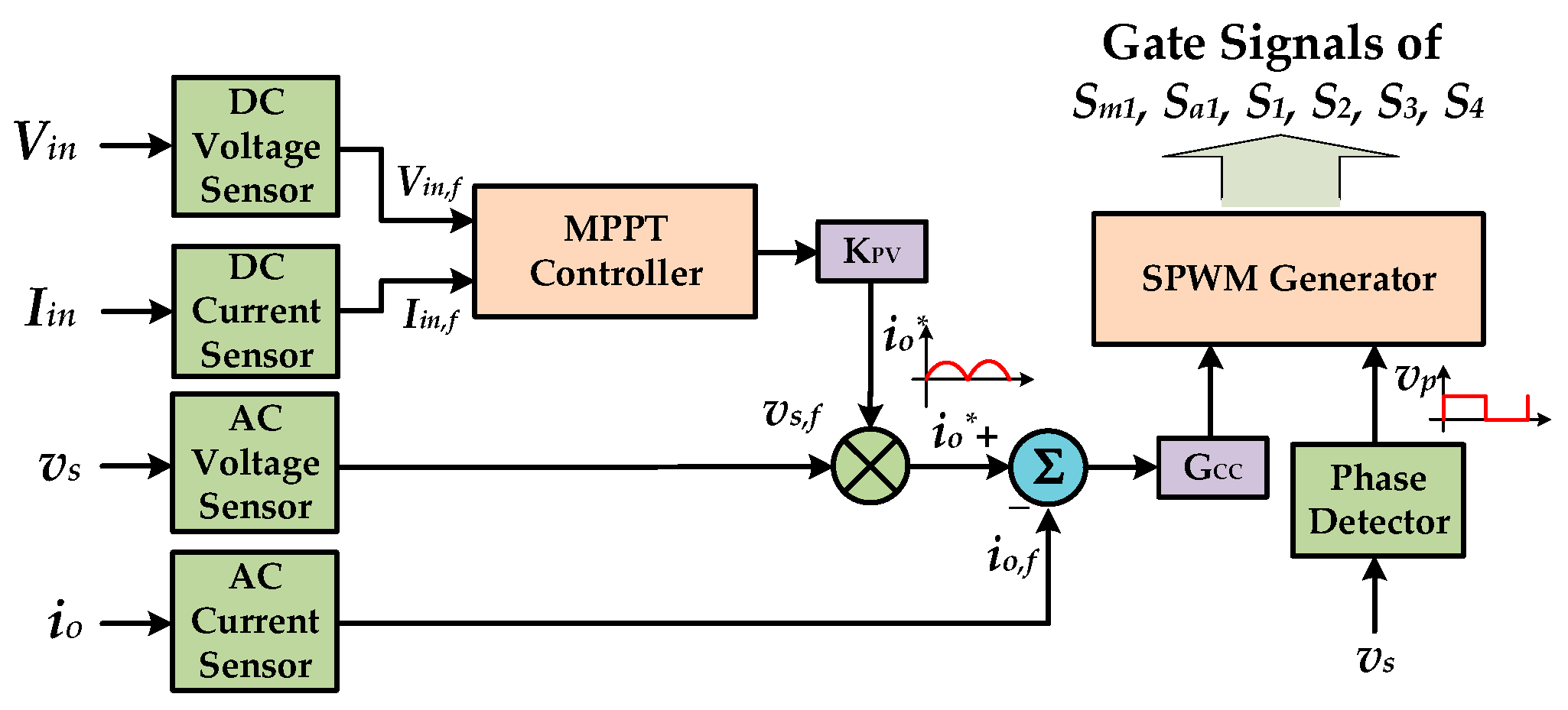
Applied Sciences Free Full Text Surrogacy Based Maximization Of Output Power Of A Low Voltage Vibration Energy Harvesting Device Html

Consider The Circuit Shown In The Figure The Current I 3 Is Equal To Img Src Https D10lpgp6xz60nq Cloudfront Net Physics Images Bms Obj Xii C03 E01 104 Q01 Png Width 80
Solved 10 Problem 10 Consider The Circuit Diagram Chegg Com
Solved 8 Problem 7 Consider The Circuit Diagram Depicted Chegg Com

Operation Of A Transformerless Three Phase Pv Inverter Using Multiple Bidirectional Choppers Yamada 2019 Electrical Engineering In Japan Wiley Online Library
Magnetic Circuit Diagram Download Scientific Diagram

Rb R Consider The Circuit Shown In The Figure Given E 5 Volts And R 1 2 Take Vo 0 Volt Re 2e 22 Ru Wh Im Er R
Solved Consider The Circuit Shown In Figure 1 2 V 2 5 A 41 Chegg Com
Glance Into Solid State Transformer Technology A Mirror For Possible Research Areas Journal Of Applied Materials And Technology

Energies Free Full Text The Short Circuit Protections In Hybrid Systems With Low Power Synchronous Generators Html
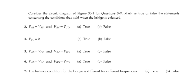
Solved Consider The Circuit Diagram Of Figure 30 1 For Chegg Com

Time Constant Calculations Worksheet Dc Electric Circuits

Consider The Circuit Shown In The Figure Below Youtube

Figure 25 Problem 2 Consider The Circuit Diagram In The 0 52 2 5 6 0 Homeworklib

In The Adjoining Circuit Diagram E 5 V R 1 W R2 4 W R1 R3 1 W And C 3 Mf Then The Numerical Value Of The Charge On Each Plate Of The Capacitance Is
Pdf Handwritten Electric Circuit Diagram Recognition An Approach Based On Finite State Machine Semantic Scholar
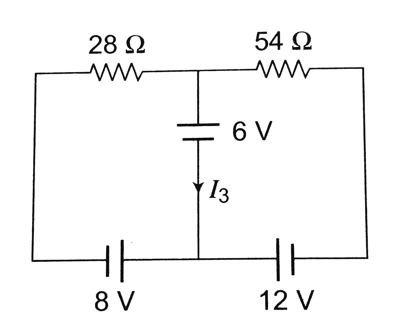
Consider The Circuit Shown In The Figure The Current I 3 Is Equal To Img Src Https D10lpgp6xz60nq Cloudfront Net Physics Images Bms Obj Xii C03 E01 104 Q01 Png Width 80
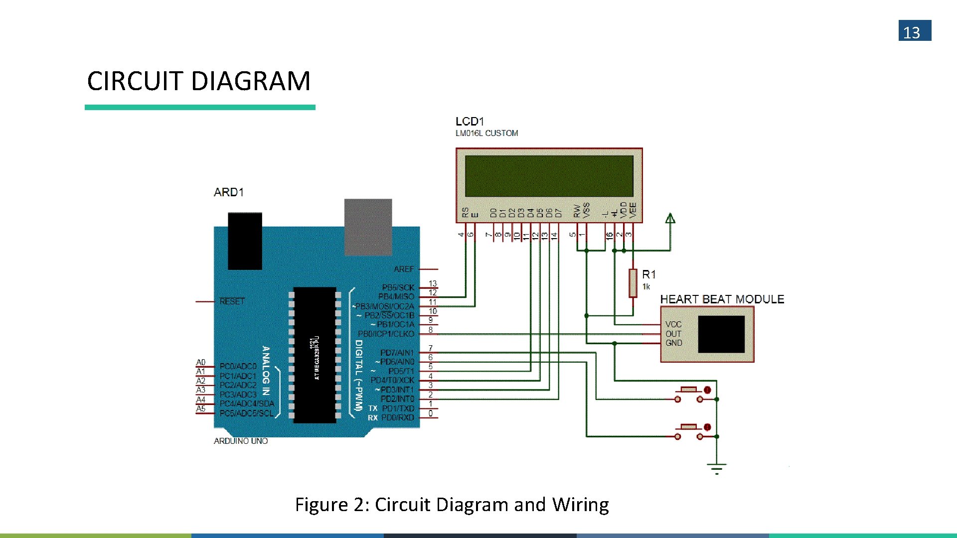
Heart Beat Monitor With Arduino First Semester Introduction

In The Adjoining Circuit Diagram E 5 V R 1 W R2 4 W R1 R3 1 W And C 3 Mf Then The Numerical Value Of The Charge On Each Plate Of The Capacitance Is
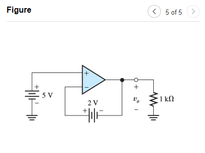
Solved Consider The Circuits Shown In Figure 1 Chegg Com

Circuit Diagram Wikipedia
0 Response to "40 consider the circuit diagram in the figure"
Post a Comment