42 p type semiconductor band diagram
p type semiconductor material - formation, properties ... Dec 02, 2021 · Energy band diagram for p-type semiconductor s; Uses of p-type semiconductors; Formation of p type semiconductor material. In a pure semiconductor crystal, each atom produces four covalent bonds with four neighbor atoms in the crystal. Now, to produce a p-type semiconductor, trivalent impure atoms like Boron (B), Aluminum (Al), etc. are needed ... Semiconductors (Electrical Properties of Materials) Part 2 They populate the conduction band of a semiconductor, thus providing a contribution to the conduction process. It has to be noted that at sufficiently high Figure 8.12. (a) Band diagram for an n-type semiconductor whose surface has been negatively charged. (b) Band diagram for a p-type...
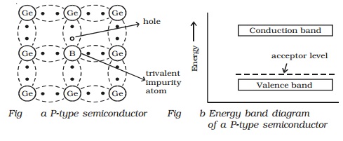
What is p Type Semiconductor? - Energy diagram and Conduction ... Energy Band Diagram of p-Type Semiconductor. The energy band diagram of a p-type Semiconductor is shown below: A large number of holes or vacant space in the covalent bond is created in the crystal with the addition of the trivalent impurity. A small or minute quantity of free electrons is also available in the conduction band.
P type semiconductor band diagram
Important Questions for CBSE Class 12 Physics Semiconductor... 11.Draw energy band diagram of n-type and p-type semiconductor at temperature T > OK. Mark the donar and acceptor energy level with their energies. 31.Write any two distinguishing features between conductors, semiconductors and insulators on the basis of energy band diagrams. PDF Semiconductor Devices | 2.5 Other Types of Diodes 47 Figure 1.14 Energy band diagram of N-type semiconductor. P-Type Material. In a similar manner, if we introduce a trivalent impurity, our crystal model now features a hole; a location where an electron is lacking. PDF 1. Semiconductor Materials & Physics | 1.3 Energy Bands Figure 1.5 exhibits the energy band diagrams of three classes of solids: insulators Similarly, for p-type semiconductors, the Fermi level moves towards the top of the valence band with increasing Conversely, in a p-type semiconductor, holes are majority carriers and electrons are minority carriers.
P type semiconductor band diagram. P Type Semiconductor: What is it? (Diagram & Explanation) We all know that in semiconductor crystal each tetra valiant atom creates covalent bond with four neighboring atoms. In this way, each of the Finally, we can say that in a p-type semiconductor has plenty of holes move randomly inside the crystal. In addition to holes generated due to trivalent... PDF Electrons and Holes | 1.3.1 Energy Band Diagram Modern Semiconductor Devices for Integrated Circuits (C. Hu). Slide 1-6. 1.3.1 Energy Band Diagram. Conduction band Band gap. Eg. If light shines on the N-type semiconductor and generates area A holes (and electrons) at the Jp(x) Jp(x + ∆x) rate of G s-1cm-3 P-type Semiconductor : Doping, Energy Diagram & Its Conduction Energy Diagram of P-type Semiconductor. The p-Type Semiconductor energy band diagram is shown below. The no. of holes within the covalent bond can be formed in the crystal by adding the trivalent impurity. A less amount of electrons will also be accessible within the conduction band. Energy Band Diagram PDF Semiconductor: Types and Band structure Types of Semiconductors Semiconductors can be classified as: · Intrinsic Semiconductor · Extrinsic Semiconductor Intrinsic Semiconductor An intrinsic type of semiconductor material is made to be very pure chemically. Energy Band Diagram for Semiconductors, Conductors, and Insulators.
1 on: "Semiconductors - Classification, Types, Band Theory" Hence in the energy band diagram of an intrinsic semiconductor, some electrons can be shown in the conduction band. The energy band structure of the semiconductor is affected by doping. The additional energy states due to donor impurities (ED) and acceptor impurities (EA) also exist in case... PDF Band Structure and Electrical Conductivity in KEYWORDS Semiconductor · intrinsic conduction · extrinsic conduction · energy band gap · conduction band · valence band · conductivity An extrinsic semiconductor, in which conduction electrons are the majority carri-ers is an n-type semiconductor and its band diagram is illustrated in... P-type Semiconductor and N-type Semiconductor and Their... Difference between P-type Semiconductor and N-type Semiconductor. We know that the p-type and n-type semiconductors come under extrinsic What is P-type Semiconductor and N-type Semiconductor? The definitions of p-type and n-type and their differences are discussed below. Introduction To Semiconductors (all content) In these E-k diagrams, often called band diagrams, plotted in what is referred to as a reduced zone scheme, the momentum that is plotted is actually a Doped semiconductors (either n-type or p-type) are known as extrinsic semiconductors. The activation energy for electrons to be donated by or...
Band diagram - Wikipedia In solid-state physics of semiconductors, a band diagram is a diagram plotting various key electron energy levels (Fermi level and nearby energy band edges) as a function of some spatial dimension, which is often denoted x. These diagrams help to explain the operation of many kinds of... PDF Basics of Semiconductor Devices | 1.1 Band Diagrams This type of semiconductor is called N type, and electrons are the majority carriers in this type of semiconductor. The above concepts are often visualised with the help of band diagrams. The arrange-ment of atoms in a semiconductor results in certain electron energies which are not permitted. File:P-Type Semiconductor Bands.svg - Wikimedia Commons File:P-Type Semiconductor Bands.svg. From Wikimedia Commons, the free media repository. Jump to navigation Jump to search. Diagram of the conduction and valence bands in a p-type semiconductor above 0K. Date. Materials Science and Engineering/Diagrams/Semiconductor Devices In solid-state physics of semiconductors, a band diagram is a diagram showing the variation in the valence band and conduction band edges vs. some If we consider a P-type semiconductor (with NA the density of acceptors, p the density of holes; p = NA in neutral bulk), a positive voltage, VGB...
What is p-type and n-type silicon? - Quora P-type and n-type silicon are basically semiconductors, which means they are neither conductors not insulators. But their conductivity lies between that of conductors and insulators. The diagram below illustrates the energy bands in intrinsic, n-type and p-type semiconductors.
Extrinsic Semiconductors: Dopants, n-type & p-type Semiconductor... An n-type semiconductor is created when pure semiconductors, like Si and Ge, are doped with pentavalent elements. As can be seen in the image above, when a pentavalent atom takes the place of a Si atom, four of its electrons The above energy band diagram is of p-type Si semiconductor.
Band Diagram - an overview | ScienceDirect Topics Energy band diagram representation of a semiconductor p-n junction. (A) With no applied bias. Figure 64 shows a band diagram of the MOS structure for thick oxides and for n - and p -type The n-type and p-type dopants were Sn and Zn, respectively, with concentrations of 7×10 18 cm −3 for...
Semiconductor, band diagram - Big Chemical Encyclopedia 4.10 Two-dimensional energy band diagram for a metal dot-coated n-type semiconductor electrode. Figure 8. Schematic representations of p-n junctions and corresponding energy band diagrams under various conditions (a) uniformly doped p-type and n-type semiconductors before...
Semiconductors - Electronics Reference | Band Diagrams Band diagrams of conductors are useful to develop an intuition of how band diagrams can be used to understand electrical properties of all sorts of materials. P-type semiconductors have many 'extra' holes that contribute to conduction. P-type dopant atoms (such as the Boron atoms added to...
Semiconductors - Engineering Physics Class In p-type semiconductor, there are no donor atoms [and hence no ions], so = 0. At 0 K, all the acceptor levels are not occupied by electrons. Figure 8.8 (a) Band diagram of n-type material at 0 K; (b) Band diagram of p-type material at 0 K. Direct and indirect band gap semiconductors.
PDF Building blocks of the pn junction theory Converting a layer of an N-type semiconductor into P type with acceptors would also create a PN junction. A PN junction has rectifying current-voltage (I-V or IV) Let us examine the band diagram of a PN junction in Fig. 4-4 in greater detail. Figure 4-4b shows that Ec and Ev are not flat.
Extrinsic semiconductor - P-type semiconductor Even though p-type semiconductor has large number of holes, but these holes is provided by the trivalent atoms that are electrically neutral. In p-type semiconductor, the population of holes in valence band is more, whereas the population of free electrons in conduction band is less.
Distinguish between n-type and p-type semiconductors on the basis The energy band diagram of n-type semiconductor has been shown in Fig. and of p-type semiconductor in Fig. From these energy band diagrams, we note that, in n-type semiconductor the forbidden energy gap is reduce by donore energy state and electrons are majority carriers.
What is P-type Semiconductor? Energy Diagram, Conduction ... In order to form a p-type semiconductor the basic step is to dope intrinsic semiconductor with trivalent impurity. In this type, the valence shell consists of three electrons requires further one more electron. This is possible by sharing the electron. As it is accepting electrons it is generally referred to as acceptor. The acceptor impurities are Boron, indium, gallium. Once these are added to either silicon or germanium p-type semiconductors are formed. Let us take boron as the trivalent impurity so that we can add it to the silicon in order to make it extrinsic. Everything here is completely based on the concept of sharing. The covalent bond concept is preferred during accepting the electrons. Boron atomic number is five. Based on its valence shell electronic configuration concept the numbers of valence electrons present in boron are three. Hence each valence electron forms a covalent bond with the neighboring silicon atoms. The number of bonds formed with a number of silicon at...
File:P-Type Semiconductor Bands.svg — Wikipedia... // WIKI 2 Diagram of the conduction and valence bands in a p-type semiconductor above 0K. File:P-Type Semiconductor Bands.svg. From Wikipedia, the free encyclopedia.
[Solved] The band diagram of a p-type semiconductor with a ... The band diagram of a p-type semiconductor with a band-gap of 1 eV is shown. Using this semiconductor, a MOS capacitor having V TH of -0.16 V, \(C_{ox}'\) of 100 nF/cm 2, and a metal function of 3.87 eV is fabricated. There is no charge within the oxide.
PDF Semiconductor Power Devices: Physics, Characteristics, Reliability Besides the E(x) band diagram of Fig. 2.2, there is the more detailed energy band representation in k-space, E(k), which allows further insight into If in a p-type semiconductor the hole current is in principle achieved by a motion of valence electrons as in the classical bubble model, the Hall constant...
2 thoughts on "Difference Between P-Type and N-Type Semiconductor" Both p-type and n-type semiconductor is the classification of extrinsic semiconductors. The major factor that generates a difference between p-type and Now, have a look at the energy band diagram of N-type semiconductor: Here, from the figure, it is clear that the existence of the Fermi level is near...
Extrinsic Semiconductors - Engineering LibreTexts Semiconductors are materials that possess the unique ability to control the flow of their charge carriers, making them valuable in applications like cell phones, computers, and TVs. An extrinsic …
PDF 1. Semiconductor Materials & Physics | 1.3 Energy Bands Figure 1.5 exhibits the energy band diagrams of three classes of solids: insulators Similarly, for p-type semiconductors, the Fermi level moves towards the top of the valence band with increasing Conversely, in a p-type semiconductor, holes are majority carriers and electrons are minority carriers.
PDF Semiconductor Devices | 2.5 Other Types of Diodes 47 Figure 1.14 Energy band diagram of N-type semiconductor. P-Type Material. In a similar manner, if we introduce a trivalent impurity, our crystal model now features a hole; a location where an electron is lacking.
Important Questions for CBSE Class 12 Physics Semiconductor... 11.Draw energy band diagram of n-type and p-type semiconductor at temperature T > OK. Mark the donar and acceptor energy level with their energies. 31.Write any two distinguishing features between conductors, semiconductors and insulators on the basis of energy band diagrams.

0 Response to "42 p type semiconductor band diagram"
Post a Comment