41 schottky diode band diagram
The effects of a Stone-Wales defect on the performance of a graphene-nanoribbon-based Schottky diode are studied herein. To this end, the transmission, energy band structure, density of states, carrier concentration, and current density of the proposed device are modeled analytically in two cases, viz. a pristine and defective graphene nanoribbon, and the results are compared. The results ...
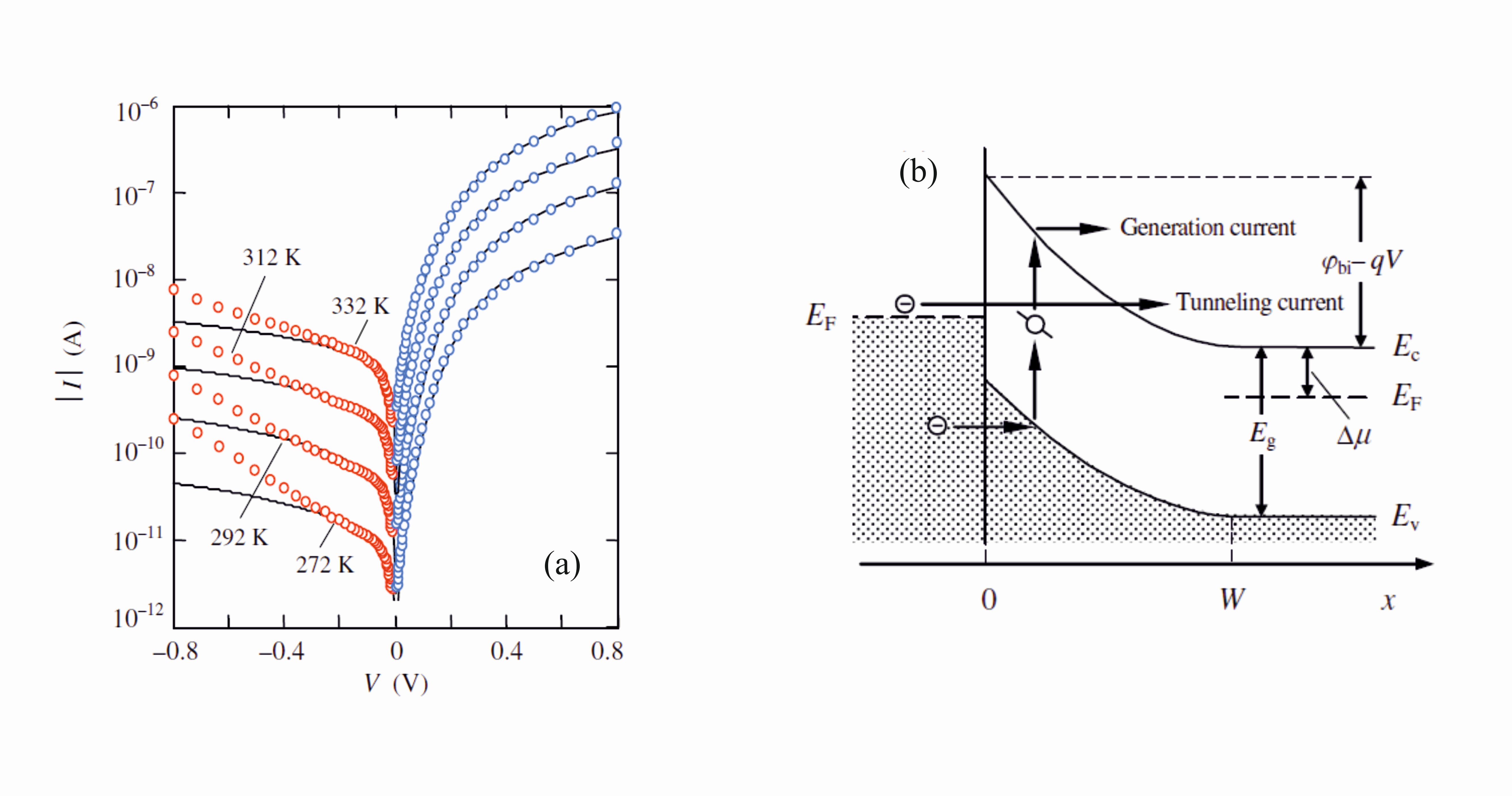
A Schottky barrier, named after Walter H. Schottky, is a potential energy barrier for electrons formed at a metal-semiconductor junction [17].Schottky barriers have rectifying characteristics, and then they are suitable for use as diodes. One of the basic characteristics of a Schottky barrier is its height, regularly denoted by Φ B (see Fig. 5.1). ...
https://www.patreon.com/edmundsjIf you want to see more of these videos, or would like to say thanks for this one, the best way you can do that is by becomin...

Schottky diode band diagram
10.2 Formation of a Schottky contact 10.3 Band diagram of a Schottky contact at thermal equilibrium 10.4 Carrier motion of a Schottky contact at thermal equilibrium 10.5 Schottky diode current-voltage characteristics 10.6 Schottky versus PN junction diodes 10.7 Ohmic metal-semiconductor contacts. 6: By the end of this week, you will be able to:
schottky diodes. Two main electrical characterization techniques were used in the investigation of these diodes, Current - Voltage Characterization and Capacitance - Voltage Characterization. Using I-V characteristics the ideality and the Barrier height of the Schottky diode was determined
Apr 22, 2011. #1. paul_harris77. 52. 0. Dear All. I am having problems with how to draw band diagrams with band bending for Schottky Barriers and PN junctions. My issue is that I don't know how you determine which Fermi level remains fixed at its equilibrium level and which Fermi level moves to align with it when the two materials are brought ...
Schottky diode band diagram.
and Schottky barrier diodes (SBDs) on different region of the same substrate have been developed to overcome the AC driving problems and achieving high breakdown voltage SBDs with high efficiency LEDs on the same wafer [1 - 7] .
2.2 Energy band diagram for Schottky contact after contact formation 15 2.3 Energy band diagram for a metal and n-type semiconductor with an interfacial layer between them 16 2.4 Response of bias voltage to a Schottky diode 18 2.5 Energy band diagram for an ohmic contact after contact formation 21 2.6 I-V curve for the ohmic contact structure 21
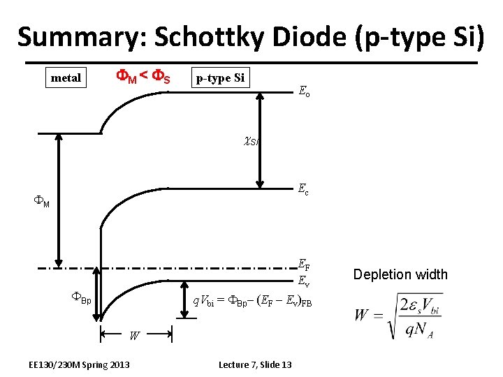
9.1 Schottky Barriers Energy Band Diagram of Schottky Contact • Schottky barrier height, φB, is a function of the metal material. • φB is the single most important parameter. The sum of qφBn and qφBp is equal to Eg. Metal Depletion layer Neutral region qφBn Ec Ec Ef Ef Ev qφ Ev Bp
Download scientific diagram | Energy band diagrams for a Schottky-PN junction diode (SPND): (a) zero bias state, (b) forward bias state, and (c) reverse bias state. from publication: A New Type of ...
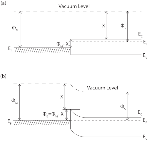
The Schottky diodes are also called hot-carrier diode, ... Schottky Diode Energy Band. In the below figure energy band diagram for N-type semiconductor material and metallic material is shown below. The energy level of electrons at the outer side of the substance is known as the vacuum level.
The schottky diode is a type of metal - semiconductor junction diode, which is also known as hot-carrier diode, low voltage diode or schottky barrier diode. The schottky diode is formed by the junction of a semiconductor with a metal. Schottky diode offers fast switching action and has a low forward voltage drop.
• Schottky Barrier/Diode ... Energy band diagram of an isolated metal adjacent to an isolated n-type semiconductor UMass Lowell 10.523 - Sanjeev Manohar. Energy band diagram of a metal-semiconductor contact in thermal equilibrium. UMass Lowell 10.523 - Sanjeev
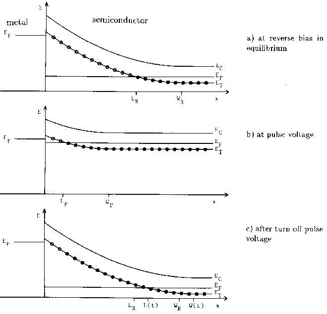
The Energy-band diagram versus voltage for the metal-semiconductor Junction shown in Fig.3 is very similar to these of the p-n junction. Because of similarity, we expect the current-voltage characteristics of the Schottky barrier junction to be similar to the exponential behavior of the p-n junction diode.
Schottky Diode I-V characteristics • Schottky diode is a metal-semiconductor (MS) diode • Historically, Schottky diodes are the oldest diodes • MS diode electrostatics and the general shape of the MS diode I-V characteristics are similar to p+n diodes, but the details of current flow are different. • Dominant currents in a p+n diode
Ⅱ Terminology 2.1 Working Principle. The Schottky diode is a metal-semiconductor device made of a noble metal (gold, silver, aluminum, platinum, etc.) as a positive electrode A, an the N-type semiconductor as a negative electrode B, and a barrier having a rectifying characteristic formed on the contact surface thereof. Since a large amount of electrons are present in the N-type semiconductor ...
Schottky diode, the fastest conventional detection technology, is a promising component for future THz communication receiver systems. However, the overall performance of ... Figure 2.1: Energy band diagram of metal-semiconductor (n-type) contact. In a) metal
Beam-lead Schottky barrier diodes are categorized by universal mixer applications in four frequency ranges: S, X, Ku and Ka bands. They may also be used as modulators and high-speed switches. Beam-lead diodes are suited for balanced mixers, due to their low parasitics and uniformity. A typical VF vs. IF curve is shown in Figure 1.
A) band scheme of a forward biased n-type schottky diode. (b ...
In a Schottky diode, the semiconductor band diagram looks very similar to that of an n-type semiconductor in a p +-n diode (compare Fig. 1a and 2). Hence, the variation of the space charge density, r , the electric field, F , and the potential, f , in the semiconductor near the metal-semiconductor interface can be found using the depletion ...

1 energy-band diagram of ms schottky diode for n-type ...
Simulation and Fabrication of Schottky Diodes and FETs based on IGZO Metal-Oxide Semiconductor A thesis submitted to the University of Manchester for the degree of ... Figure 1.2(a): Energy band diagrams for Schottky contact on n-type semiconductor and
Current-voltage characteristics of silicon carbide ...
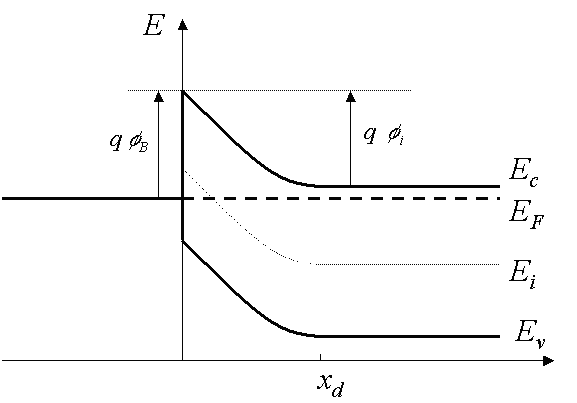
3. 1. 6. 2 Schottky Contact A Schottky barrier refers to a metal-semiconductor contact having a large barrier height (i.e. and low doping concentration that is less than the density of states in the conduction band or valence band. The potential barrier between the metal and the semiconductor can be identified on an energy band diagram.

Schottky diode - an overview | sciencedirect topics
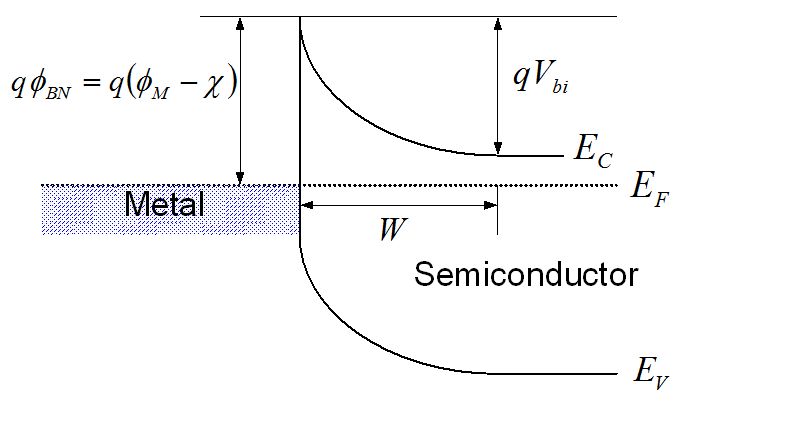
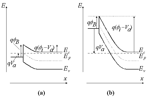
Figure V.4. The energy diagram for a Schottky barrier diode, ϕ Bo is the barrier energy, qϕ Bo is the barrier voltage, qϕ Bn is the effective barrier voltage including image forcing lowering, and ξ is the energy difference between the bottom of the conduction band, E c, and the Fermi level.

Line 22f1fa19c3m1b7c8e13c9c6a schottky junction solar ...
Energy band diagram of schottky diode. The energy band diagram of the N-type semiconductor and metal is shown in the below figure. The vacuum level is defined as the energy level of electrons that are outside the material. The work function is defined as the energy required to move an electron from ...
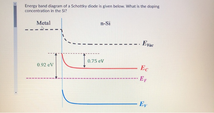
Solved energy band diagram of a schottky diode is given ...
Schottky diode Draw the band diagram (valence band, conduction band, Fermi energy) for a Schottky diode with a n doped semiconductor and a p doped semiconductor at zero bias. Assume that interface states pin the Fermi energy to the middle of the semiconducting gap at the interface.
Implementation of schottky barrier diodes (sbd) in standard ...
A Schottky barrier, named after Walter H. Schottky, is a potential energy barrier for electrons formed at a metal-semiconductor junction.Schottky barriers have rectifying characteristics, suitable for use as a diode.One of the primary characteristics of a Schottky barrier is the Schottky barrier height, denoted by Φ B (see figure). The value of Φ B depends on the combination of metal and ...

Schottky barrier - wikipedia
Let's see the diagram of the energy band of Schottky diode: Schottky diode Characteristics Curve. Now, let's discuss the voltage and current characteristics of the Schottky diode. It has low forward voltage loss that's why its characteristic curve is close to current axes as compared to normal diodes.

Schottky diode - definition, symbol, working and applications ...
The Schottky diode (named after the German physicist Walter H. Schottky), also known as Schottky barrier diode or hot-carrier diode, is a semiconductor diode formed by the junction of a semiconductor with a metal. It has a low forward voltage drop and a very fast switching action. The cat's-whisker detectors used in the early days of wireless and metal rectifiers used in early power ...

Schottky barrier - an overview | sciencedirect topics
Schottky diode Draw the band diagram (valence band, conduction band, Fermi energy) for a Schottky diode with a n doped semiconductor and a p doped semiconductor at zero bias. Assume that interface states pin the Fermi energy to the middle of the semiconducting gap at the interface. Indicate where the depletion region is and explain why it is depleted. ...

Schottky diode part 1 - band diagram
Download scientific diagram | Energy band diagram of a metal-semiconductor Schottky diode with a p -doped quantum well, ͑ a ͒ without bias and ͑ b ͒ with forward bias. E c from publication ...

Schottky.t

Schottky barrier - wikiwand
Schottky diode
Schottky diodes heterojunctions and ndr diodes

Figure 1 | optimum barrier height for sic schottky barrier diode

Ee327 lec 22c schottky
Description of transport properties of schottky diodes ...
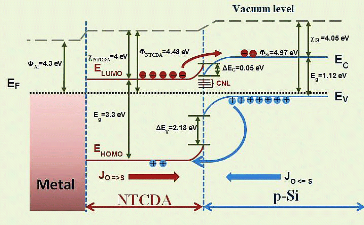
Figure 15 | analyzed electrical performance and induced ...

Modeling electrical properties of organic schottky diodes ...
1. schottky diode
Schottky barrier
Flexible indium–gallium–zinc–oxide schottky diode operating ...
Schottky diode
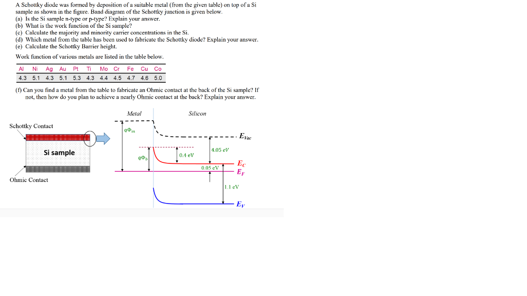
Solved a schottky diode was formed by deposition of a | chegg.com

A) energy band diagram of back-to-back schottky diodes with a ...

☑ forward biased schottky diode

Energy band diagram of schottky diode with n-type base and qw ...
Schottky diode

Ee327 lec 22e schottky

Metal-semiconductor-metal heterojunction diodes consisting of ...

Energy band diagram of schottky diode with n-type base and dl ...

Penghalang schottky - wikipedia

Schottky diode - definition, symbol, working and applications ...

7 band diagram of trap modulation in a n-type schottky diode ...

Schottky barrier diode - power microelectronics. device and ...
Schottky diodes heterojunctions and ndr diodes
Schottky diode
3.1.6.2 schottky contact
Metalsemiconductor contacts there are 2 kinds of ...
0 Response to "41 schottky diode band diagram"
Post a Comment